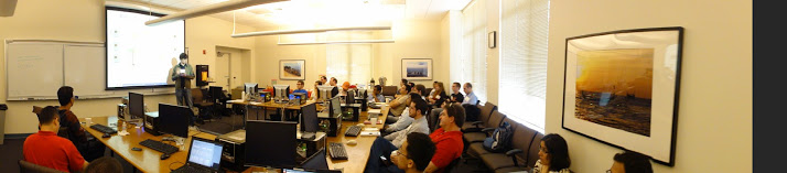
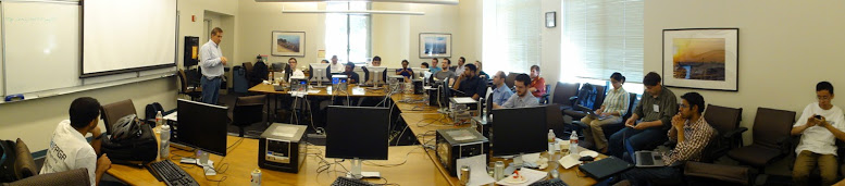
NetFPGA Summer Camp 2013
Build an internet router and learn about clean-slate switches at a 5-day summer camp held at Stanford University
Open to: Academics teaching classes with the NetFPGA, and researchers (postdoc or graduate-student) interested in developing new hardware-accelerated network application
Location: Gates Building, Room 415, 353 Serra Mall, Stanford, CA 94305
Dates: Monday, July 29th - Friday, August 2 2012
Time: 9am - 5pm
Presented by: the Stanford NetFPGA Group.
Abstract
An open platform called the NetFPGA has been developed at Stanford University. The NetFPGA platform enables researchers and instructors to build high-speed, hardware-accelerated networking systems. The platform can be used in the classroom to teach students how to build Ethernet switches and Internet Prototcol (IP) routers using hardware rather than software. The platform can be used by researchers to prototype advanced services for next-generation networks.
By using Field Programmable Gate Arrays (FPGAs), the NetFPGA enables new types of packet routing circuits to be implemented and detailed measurements of network traffic to be obtained. During the tutorial, we will use the NetFPGA to determine the amount of memory needed to buffer TCP/IP data streaming through the Gigabit/second router. Hardware circuits within the NetFPGA will be implemented to measure and plot the occupancy of buffers. Circuits will be downloaded into reconfigurable hardware and tested with live, streaming Internet video traffic.
Background
Attendees will utilize a Linux-based PC equipped with NetFPGA hardware. A basic understanding of Ethernet switching and network routing is expected. Past experience with Verilog is useful but not required. This week-long summercamp extends the material presented at the shorter workshop events.
Slides
Day 1: ppt
Outline
Day 1 (Monday, July 29)
- Welcome and Introductions
- NetFPGA
- Infrastructure
- Tree
- Build System
- Scripts
- Life of a packet through the NetFPGA
- Data and control planes
- Interface to software: Exceptions and Host I/O
- Implementation
- Module Template
- User Data Path
- Write crypto NIC using a static Key
- Simulation and Debug
- Simulation functions
- Write and Run Simulations for crypto NIC
Day 2 (Tuesday, July 30)
- NetFPGA (cont.)
- Registers
- Explain Register System
- Add XML to define crypto NIC encryption key
- Use Generic Register Module to implement register
- Update Simulations
- Build and Test Hardware
- Build
- Explanation of Hardware Tests
- Write and run Hardware Tests
- Verify value: 0xFFFFFFFF
- Verify value: 0xFF00FF00
- Verify value: 0x55555555
- Writing Software and Integration
- Write setkey.c/getkey.c to write/read registers
- Test between adjacent computers
- Group Discussion
- Projects ideas
- Scope of work that can be accomplished in 2-3 days
- Team up for Projects
- Project leaders will describe projects
- Group will provide feedback on the scope
- Be sure to have one hardware designer per team
- Example Hardware Design
- Background and review of block diagrams
- Show design running on nf-test machines
- Discuss relevant Verilog Code
Day 3 (Wednesday, July 31)
- Work on Projects, examples from Summer Camp 2008 & 2010
- 802.1q VLANs
- Hardware-Accelerated Mathematics Library for NetFPGA
- MACinMAC
- Heavy Hitter Identification using Multistage
- Layer 2 Load Balancing
- Pattern Matching/Mini-IDS
- TCP Traffic Analysis for Passive End-to-End Bandwidth Measurement
- Assessment of Prototyping an AFDX Policy Switch Leveraging NetFPGA, Ethane, and OpenFlow Switch
- ntop on NetFPGA
- Universal Hash Function
- NetFPGA group available for Questions and Answers
- Dinner: TBD
Day 4 (Thursday, Aug. 1)
- Complete Projects
Day 5 (Friday, Aug. 2)
- Complete Projects
- 10-minute project presentations
- Live demonstrations
- Award prizes to winning projects
- Dinner: TBD
Background Reading
- NetFPGA Website
- EDK Tutorials
- NetFPGA Projects
- The Verilog Golden Reference Guide, by Doulos
To Attend this Event
- Mark your calendar with the dates of the event
- Please plan to arrive Sunday night July 28
- Please plan to stay through Saturday morning, August 3
- Registration fee covers shared meals (all breakfasts, lunches, and most dinners)
- Registration Fee:
- Early (before June 15th): $250
- Late (after June 15th): $350
- Register: Registration Site
- Registration Deadline: July 6th
- A limited number of scholarships are available for students or instructors unable to cover registration and hotel expenses. Scholarship applicants do not need to register through the registration website.
- Award of the scholarships will be based on both merit and need:
- Please provide one paragraph about that describes your relevant technical background in networking and/or hardware design.
- Please provide another paragraph that explains why you or your host institution needs financial help.
- Scholarship Application:
- Travel Information
- Direct flights are available to most parts of the country through SFO and SJC
- CalTrain offers fast transportation between the airports and Palo Alto
- The Marguerite Shuttle offers rides between the train station, hotel, and campus. No car rental is needed.
- Hotel information coming soon